- RESEARCH INFRA
- Special Theme _ SEMICONDUCTOR
본문영역
Future of regional-based
semiconductor public FAB
-
UNIST Central Research Facilities
Nano Fabrication Center
Semiconductors are the most important materials in smart technologies represented by AI and self-driving cars. The UCRF, which was founded along with UNIST’s founding in 2009, has continuously built a system to support overall semiconductor processes. Among them, the “UNIST Nano Fabrication Cleanroom (UNFC)” is the key organization in semiconductor production, serving as a reliable base of R&D support in semiconductors, as it has been extended to an area of 1,000㎡ in 2017.
UCRF and UNFC support the leading-edge research
UCRF was founded to support the R&D of UNIST members. It has installed expensive high-tech equipment required for the highly advanced fusion research, which supports UNIST members to jointly use them, and arranges for specialized technical manpower to manage that equipment. UCRF, where the best equipment and technical staff are gathered, are supporting services such as testing, analysis, and processing with the service range extended to regional industrial companies, research centers, and universities.
Currently, UCRF holds more than 300 pieces of research equipment. Its supporting fields consist of the “Nano Fabrication Center” for nano-processing, the “Materials Characterization Lab” to analyze material characteristics, the “Design & Manufacturing Center” to fabricate various experimental devices and process precision specimens, the “Environmental Analysis Center” to analyze an extremely small amount of pollutants in the environment, the “Optical Biomed Imaging Center” to view changes in live cells and entities in real time, the “In Vivo Research Center” to verify bio-efficacy verification research using bio-convergence technology, and the “Radiation Safety Lab” to manage and supervise radioactive materials and equipment and radiation workers. The shared equipment in UCRF is freely used by researchers according to the autonomous equipment use scheme. To make this scheme more efficient and effective, UCRF provides continued education and seminars on how to use equipment and analyze results.
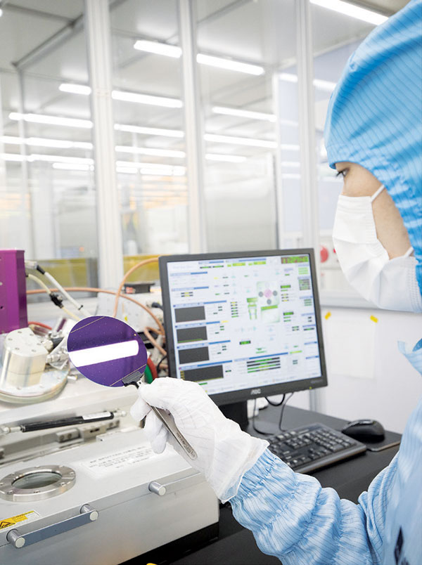
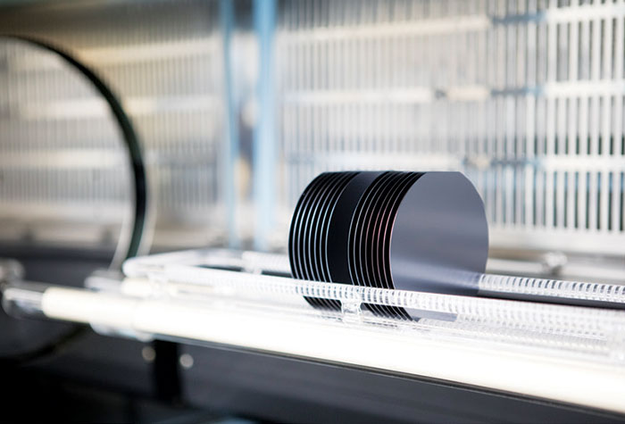
The UNIST Nano Fabrication Cleanroom (UNFC) installed inside UCRF was launched as a form of laboratory scale that manufactured mainly metal pads in 2009. Currently, it is run as a fabrication (FAB) facility that develops and researches memory (dynamic random access memory & NAND flash) and non-memory systems.
UNIST Nano
Fabrication Cleanroom
FAB, the key to the semiconductor manufacturing industry
The semiconductor industry is largely divided into either design and development or manufacturing. Some of the representative fabless companies that mainly focus on design and development are Apple, Qualcomm, NVIDIA, REALTEK, etc. Some of the representative manufacturing companies, which are foundries that are responsible for wafer chip manufacture, are TSMC, SMIC, and UMC. There are integrated device manufacturers (IDM) that oversee all processes in producing semiconductors from design to manufacture, namely Samsung Electronics, SK Hynix, and Intel.
The criterion that divides design and development and manufacturing is whether there is a FAB, or foundry. It is difficult to maintain and operate a FAB because it requires micro-processing technology and capital investment. Some IDMs are shifting more toward outsourcing fabrication because of this difficulty. These are called FAB-light companies. As such, a FAB is positioned very importantly in the semiconductor industry. Although it is called “outsourcing manufacture,” this is different from the contractor-subcontractor system in existing industries. The relationship between design and development and manufacturing should be viewed as collaboration because it would be useless if the foundry stage could not perform manufacturing even if a groundbreaking technology in semiconductors is developed.
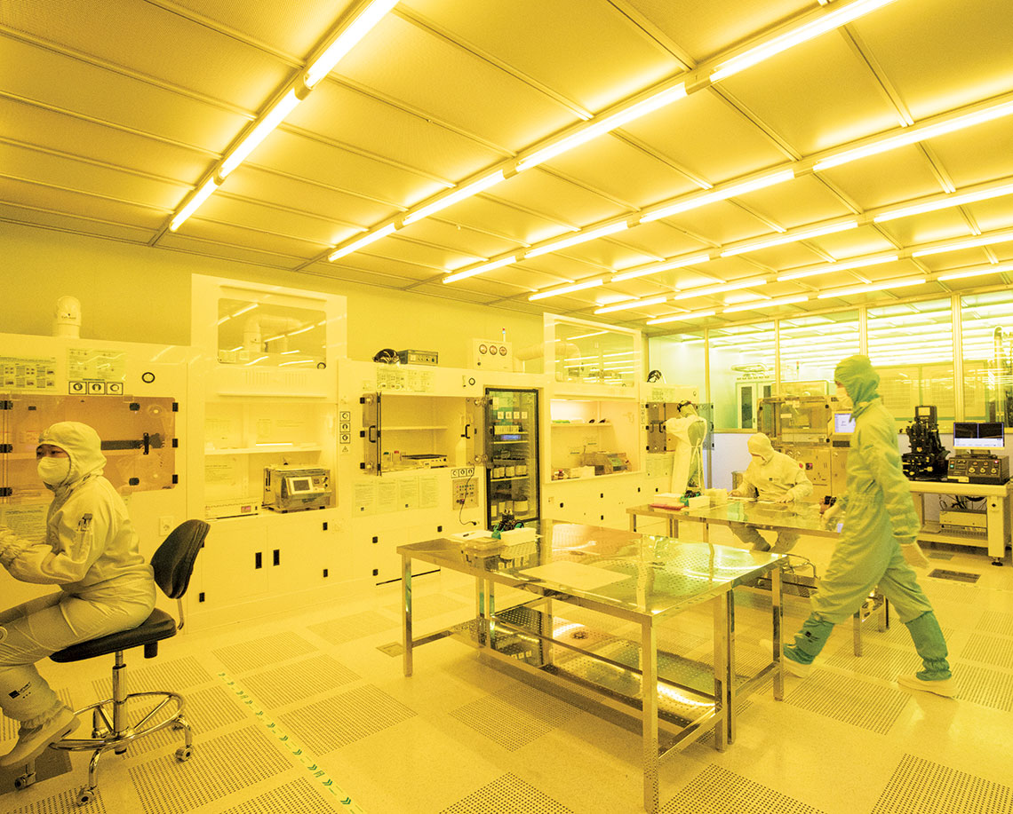
The most important technology in FABs is “nano processing.” Facilities like a cleanroom should be set in place because semiconductor chips are manufactured at a nano-meter level. The UNIST Nano Fabrication Center has also achieved investments and growth based on such infrastructure. Although our center is different from other large FABs that are run with large-scale investment, it has been expanded and transformed into a 1,000㎡ super cleanroom in 2017 thanks to ongoing investment in equipment and manpower recruitment every year and a 150-nanometer NAND flash-based GAA device in development.
This growth has been driven by the semiconductor researchers and the key material and device development platform at USNIT. It is also due to the development of professional manpower in semiconductors and the continuous support to develop pilot products as its infrastructure is run as a research institution as originally intended.
Managed by experts and autonomously used by users
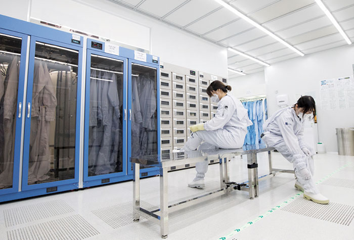
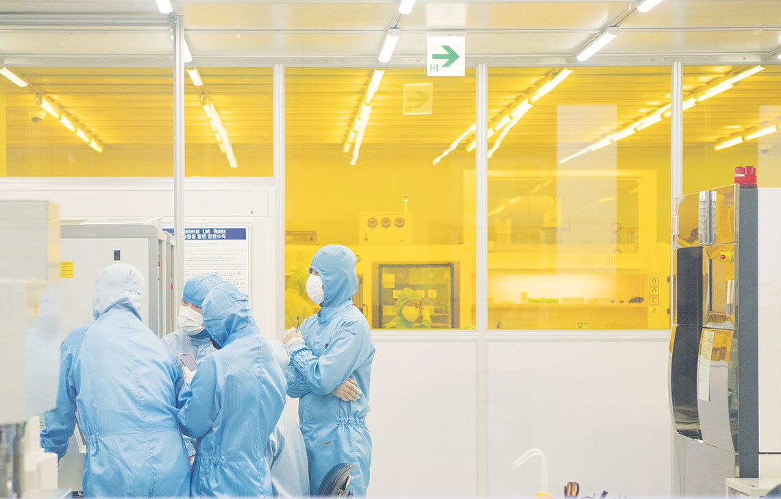
UNFC boasts its own professional manpower for efficient and safe operations. An efficient FAB environment has been maintained based on their expertise in each area, specifically one expert in process integration, two in the lithography process, two in the etching process, and four in the thin film process. In addition, the temperature, humidity, and the amount of dust must be constantly managed every day all year-round in the semiconductor FAB. Thus, heating, ventilation, and air conditioning are running constantly in invisible places and filter management is set in place. In particular, since equipment in UNFC is used by many researchers for various purposes, breakdown maintenance is frequently conducted. To cope with this, a maintenance specialist (manager) is stationed at the center to respond to a breakdown in real time and conduct preventive maintenance activities.
The autonomous equipment use scheme in UCRF is maximizing the equipment use efficiency. Autonomous users are produced through the monthly equipment manual training. Not only simple equipment usage but also recipe and process know-how are passed on to those who are equipped with a certain level of competence, so that they can freely manufacture their preferred semiconductor devices according to the preset rules.
The equipment manual training is part of the response manual on safety-related accidents. The risk of safety accidents is always present in the UNFC processes because toxic gases, strong acid, base solutions, etc. are used. This is why the equipment should be used after expertise on how to correctly use the equipment is ensured. Improving the safety awareness of users is important but systematic improvements should also be undertaken. Accordingly, explosion-proof gas cabinets, emergency ventilation systems, personal protective equipment, and emergency response measures (i.e. safety items such as body/ eye shower facilities, anti-chemical creams, solution fences, etc.) are closely situated.
The goal is a “No. 1” semiconductor research FAB facility.
Major semiconductor FABs in South Korea are in fact concentrated in the Gyeonggi and Chungcheong regions. It takes more time to build infrastructure in the Gyeongsang region where UNIST is located because only recently the semiconductor industry has been actively progressing with the development of semiconductors for vehicles and power semiconductors. In line with this circumstance, UNIST is searching for ways to play the role of a regional-based public FAB in various ways.
The semiconductor industry is growing fast so it requires timely investment in equipment, and also requires manpower who can efficiently run the invested equipment. To do this, UNFC will continue the effort to secure operating manpower in proportion to ongoing investments exceeding KRW 1 billion every year and the FAB input cost.
The semiconductor device industry is a progressive field where all the latest technologies are integrated, so it requires new technological development. Alternatively, it is also a conservative industry because it has tended to stick to proven device operation schemes or used materials and components in the past. To overcome this limitation and achieve innovative performance, the FAB installed in UNIST as a research institution has much more advantageous conditions than large FABs. Thus, we aim to focus more on research on device fabrication of various structures and research on semiconductor-geared key materials and components with the purpose of “Beyond Silicon (Si).” UNFC has significantly grown every year since its founding in 2009. Nonetheless, it has an obvious limitation in competition with large research FABs. It needs to solve the shortage of operating manpower or the relatively loose organizational capability to respond to semiconductor-related policies or projects independently. However, we have sufficient competitiveness if we fully levereage our strengths at UNIST such as forming semiconductor process infrastructure and developing specialized manpower. In addition, we will make every effort to expand public benefits as a government-funded research institution and regional-based facility.