- LABORATORY
- Special Theme _ SEMICONDUCTOR
본문영역
The foundation of the next-generation
semiconductor development is formed.
-
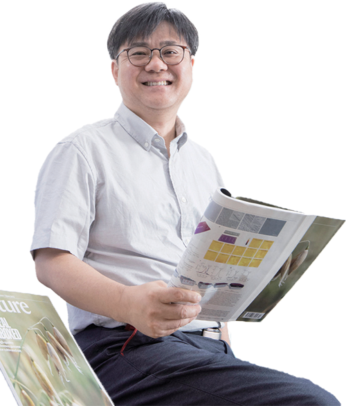
Team of Professor Hyun Seok Shin in the Department of Chemistry
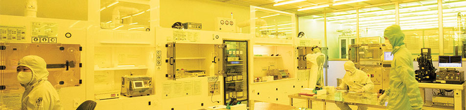
The challenge to increase the micro-device integration density that determines semiconductor performance is ongoing.In particular, the development of semiconductors with 2D materials has been successively attempted instead of 3D materials, which reached the limits of miniaturization and integration density. To do this, it requires the technology to produce high-quality 2D insulators at a preferred thickness, which are inserted between the 3D substrate and 2D material. Professor Hyun Seok Shin in the Department of Chemistry has developed a technology capable of synthesizing multiple layers of hexagonal boron nitride, the only 2D insulator, in the form of a single crystal thin film for the first time globally, charting the technological path of next-generation semiconductors.
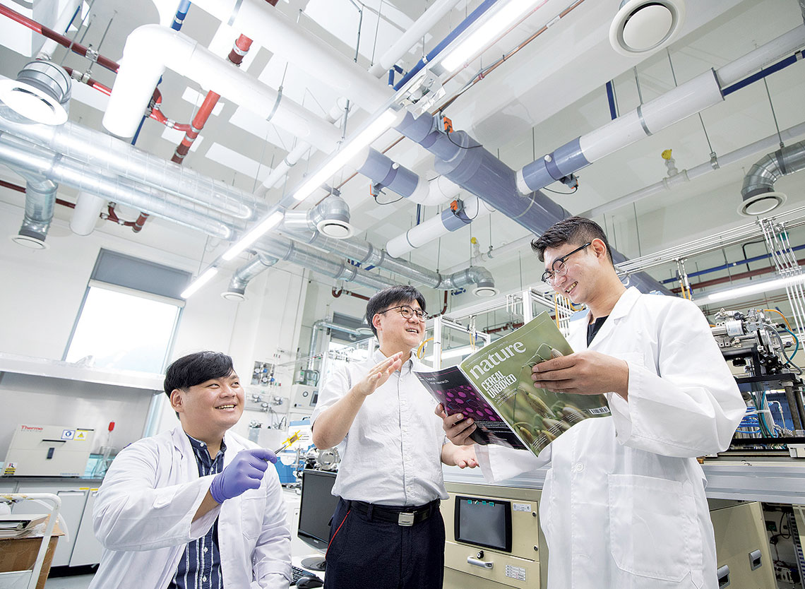
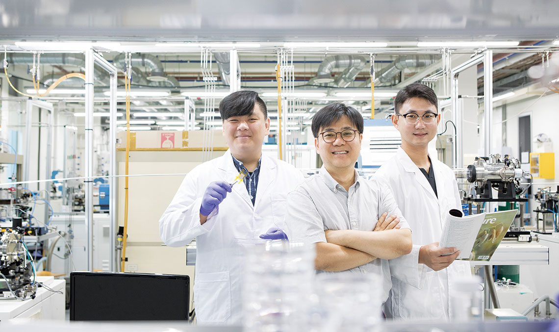 From the left, Hyeong Joon Kim (Ph.D. candidate), Professor Hyun Seok Shin, and Min Soo Kim (Ph.D. candidate)
The emergence of 2D materials that can replace silicon
Semiconductors have advanced at a breakneck speed over the past decades. The prediction of Gordon Moore that the integration density of microchips will double roughly every 24 months was nearly correct. Thus, it was called Moore's Law, which represents the rapid technological growth in the semiconductor industry. However, Moore's Law seems slowly obsolete when we see the current semiconductor development status.
One semiconductor chip contains billions of micro-devices (transistors). To increase the semiconductor performance, micro-devices should be smaller and thinner to be fit more in a chip. However, silicon made of 3D materials has a fatal problem that degrades the semiconductor performance and life, such as short channel effect and charge scattering, which causes transistor damage due to current leakage and heating as it becomes smaller. This is because of the dangling bond, which is an incomplete chemical bond at the surface while processing the silicon surface.
To solve this problem, the semiconductor industry has researched the use of 2D materials such as molybdenum disulfide (MoS2) instead of using 3D material silicon. The short channel effect and charge scattering, which are found when 3D materials are made smaller, do not occur in 2D materials because their composition atoms are connected in a plane form. Thanks to this, the micro-device integration density and semiconductor performance can keep improving using 2D materials.
The world's first technology that accelerates the commercialization of 2D insulators
There is one more problem to be solved when 2D materials are used as micro-devices instead of silicon. A wafer, a substrate on which micro-devices are laid, is also made of silicon. Thus, 2D material and wafer should be separated by an insulator to make semiconductors made of 2D materials to exhibit their function. Here, the insulator should also be made of 2D materials. If the insulator is made of 3D materials, it cannot avoid a dangling bond.
Hexagonal boron nitride (hBN) is a unique 2D insulator material, which is known to date, and can prevent semiconductor functional degradation problems, such as charge trap or charge scattering. Its molecular structure is similar to that of graphene, but its color is white, which is also called “white graphene.” To use hBN as a 2D insulator, it should be synthesized into a single crystal structure where the entire crystal is regularly generated along a certain crystalline axis. Previously, there were cases of synthesis of a single crystal of hBN whose size can be commercialized, but the thickness of all of them was a layer of the atom, which could not function as an insulator.
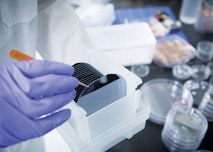
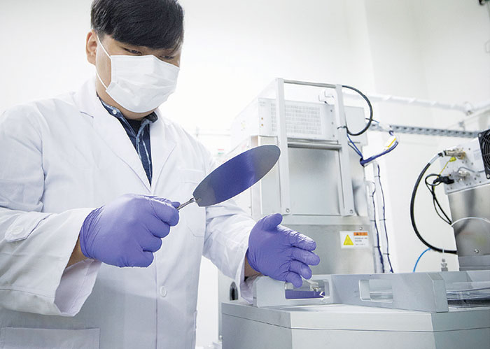
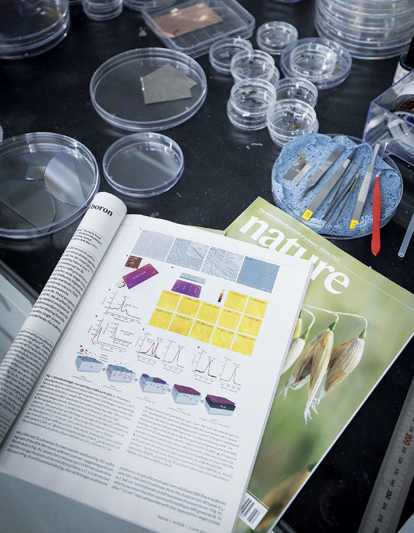
The synthesis of hBN developed by the team led by Professor Hyun Seok Shin in the Department of Chemistry is a breakthrough technology that can stack single crystal hBN thin films in multiple layers. It is the world's first synthesis technology that can make a single crystal hBN thin film at a preferred thickness while finely adjusting the concentration of the raw material on the nickel substrate. The paper titled 「Epitaxial single crystal hexagonal boron nitride multi-layers on Ni(111)」 that showed this research achievement was published in the global academic journal Nature on June 2, 2022.
Contribution to the innovation of semiconductors with relentless challenge-taking
The synthesis method of single crystal multi-layer hBN thin film developed by the team led by Professor Hyun Seok Shin is not just a coincidence. Professor Shin has steadily conducted a study on the synthesis and application of hBN since 2012. In 2020, he disclosed that amorphous boron nitride, which is a kind of boron nitride, is an ultra-low dielectric material that prevents the signal transmission delay in high-density semiconductors, and published this research achievement in the journal Nature.
“Amorphous boron nitride was discovered in 2018 when I studied hBN. Its dielectric constant was very low at 2.0 or lower so I found it could be used as a dielectric that blocked electrical interference when semiconductors were miniaturized during my research for two years. Since then, research and development have been conducted on the commercialization of amorphous boron nitride by many semiconductor companies. We expect that the synthesis method of single crystal multi-layer hBN thin film will play a significant role in improving semiconductor technology.”
We were successful in synthesizing single crystal hBN thin film at multiple layers, but for commercialization, we still need one more technology to be developed. That is a technology that transfers an hBN thin film synthesized on a nickel substrate onto a wafer without damage. The Professor Shin’s team is now also spurring research on this. Professor Shin added, “Once this technology is developed, it can be used to transfer not only hBN thin films but also various 2D materials.”
Professor Shin’s team plans to widen its research even on application chemical areas using hBN in addition to the foundational research related to hBN. We hope their efforts will lead to the innovation of semiconductors.
An innovative future heralded with hexagonal boron nitride MINI INTERVIEW
-
Professor Hyun Seok Shin in the Department of Chemistry
-
- Q. Please tell us about your motivation for the study of hBN. I have developed many courses and built research infrastructure after I came to UNIST in July 2008 and then I started research on 2D materials. It was about graphene, which was the biggest issue at that time. A lot of research has already been done on this subject. So, I decided to engage in more research geared to challenge-taking, being my impetus to start the research on hBN in 2012.
- Q. What is your research motto as a leader of the research team? I have a motto that always tells my research team members. In short, “Let’s pursue pioneering research beyond the conventional standards.” I said this many times in the sense of pioneering a new research field that can innovate the world, relentlessly taking on challenge to the fullest, and creating results surpassing any field that many other researchers are already vested in. The amorphous boron nitride published in “Nature” in 2020 and the synthesis method of single crystal multi-layer hBN thin film published this time are valuable achievements with this research mindset geared to challenge-taking.
- Q. Please tell us about the current project and future research plan. We are researching the synthesis of single crystal hBN multi-layer thin films on inexpensive substrates instead of expensive nickel substrates. We are also continuously researching a technology to transfer a thin film synthesized on the substrate to a wafer without damage. We have established a venture company called “Nexterials” at the university. From here, we also conduct applied research to use hBN in various ways including hydrogen fuel cell electrolyte membranes, next-generation secondary battery electrode materials, quantum light source, etc. We will endeavor to research relentlessly to deliver innovative impact on many latest industrial sectors including the semiconductor industry.