- RESEARCH INFRA
- Special Theme _
NATURE INSPIRED TECHNOLOGY
본문영역
Microanalysis and scanning electron microscopy,
--
the key elements of nature simulation technology
The importance of being fully equipped with the necessary equipment in any field is best summarized by the expression “Everything depends on the equipment!” The same goes for research. UNIST’s Central Research Facilities Center (UCRF) is equipped with research equipment comparable to that of any other research institution. In particular, since most recent research takes place at the nanoscale, the rate of utilization of equipment such as microscopes is very high. The typical research in this area is biomimetics technology, which mimics the structure or principles of living organisms or biomaterials in nature, such as animals and plants, and applies them to technology. UCRF systems, such as a scanning electron microscope capable of high-magnification microstructure analysis, are utilized in this study.
Start by taking a good look
It would not be an exaggeration to say that new technology begins with “imitation” as the creation of something from nothing rarely happens. In most cases, new technology is born as a motif based on an experience of seeing or touching something. General Yi Sun-shin’s turtle ship, with which we are of course very familiar, is a representative example of imitation technology. The designers of the ship sought to imitate both the shape of a turtle with a hard shell and its characteristic of pushing out and pulling in its neck (cannon), thus creating a battleship with an unprecedented form. In addition to examples of imitating shapes, many technologies have been developed by mimicking the properties or characteristics of materials. Velcro, commonly referred to as “squeekie” in Korea, was created by copying the shape of a hook after observing that thistle or cocklebur fruit adhere well to animal fur or clothing. Moreover, in the case of Japan's bullet train, the Shinkansen, the front part of the train was designed to mimic a kingfisher so as to reduce air resistance.
The core of this imitation starts from looking closely at something, in other words, from observation. To find out why a given substance or phenomenon reacts in a certain way, it is necessary to observe it very closely. In the past, the motif was a phenomenon visible to the human eye, such as a turtle ship, but as science gradually developed, it became possible to examine phenomena with a minute size of a few hundreds or even just a few tens of nanometers (nm) and discover more characteristics and components, leading to various technological developments.
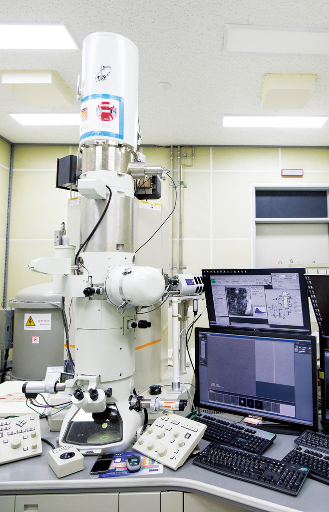
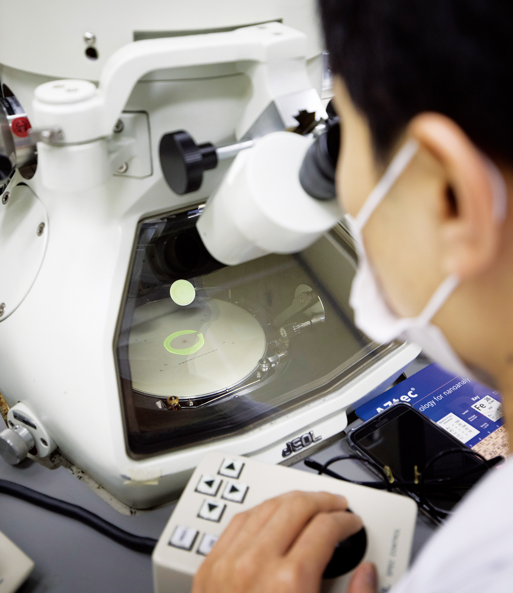
Scanning electron microscope for looking into microstructures
It is reported that the resolution at which human eyes can distinguish objects is about 0.1 millimeters (mm), which may be thought of as being equivalent to the thickness of a human hair. Equipment such as an optical or electron microscope is necessary to observe something smaller. Electron microscopes include scanning electron microscopes (SEM) and transmission electron microscopes (TEM). The SEM is mainly used to observe the microstructures on the surface of specimens at a high magnification, while the TEM is primarily a device for observing the internal structure of a specimen at a high magnification.
This issue focuses on the SEM as it is one of the leading instruments used in the biomimetics technology described above. In particular, SEMs are highly versatile in most research fields, such as materials engineering, semiconductors, life sciences, and food science.
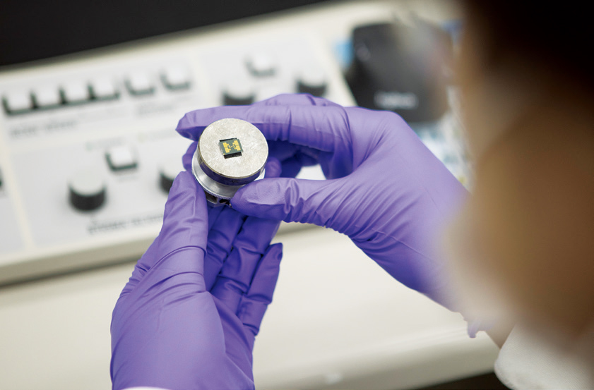
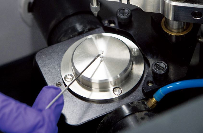
An SEM can be used to check the microstructure on the surface of a specimen with a high-magnification image, and is capable of performing everything from checks of a material’s shape to the analysis of components. In addition, since it is a surface analysis system, it can measure any solid specimen. It can measure a specimen with a size of about 1 millimeter or smaller in width and length, and can convert into images the signals obtained by continuously injecting an electron beam (e-Beam) into the specimen during the scanning process. It can also measure the surface of non-conductive materials, such as polymers and biomaterials, after a separate pretreatment process*.
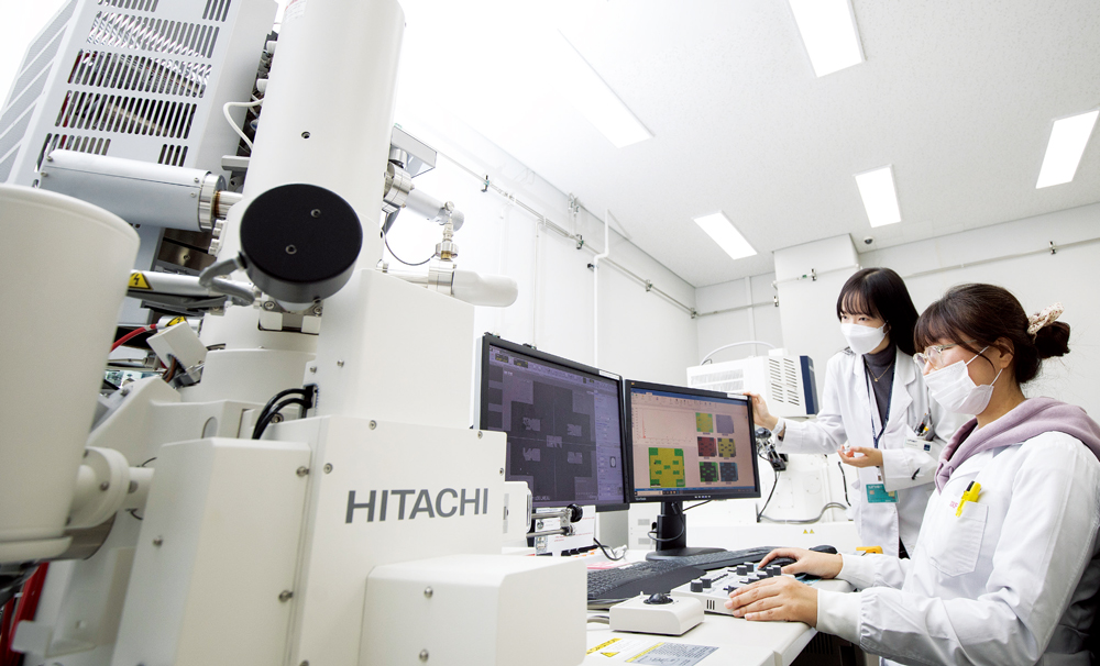
Currently, we have five SEMs in the UCRF instrument analysis room and two in the nanodevice processing room. We also has various auxiliary devices, such as the EDS, which is capable of analyzing the main components, and the WDS, which can analyze high-resolution trace element components. UNIST students and researchers who have passed the autonomous user training program can reserve and use the equipment 24 hours a day, 365 days a year.
The reason why we have such a large number of scanning electron microscopes is because, as mentioned above, they are widely used in a variety of fields. For example, when making a semiconductor device, specific materials are deposited on a wafer, so it is necessary to check whether the deposition is proper and how many nanometers of deposition will result in the best performance. However, as with most experiments, it is rare for a single test to yield sufficient results. The process of making and checking has to be repeated, but since we have multiple units, we can use them as often as we want without having to wait. In other universities and research institutes, scanning electron microscopes are used frequently, but as they generally only have one or two units, researchers have to wait anywhere from one to three months just to use them once. Since these differences also affect the progress of research, it can be seen that they also contribute significantly to UNIST's research outcomes.
The UCRF specialty that enhances the quality of research
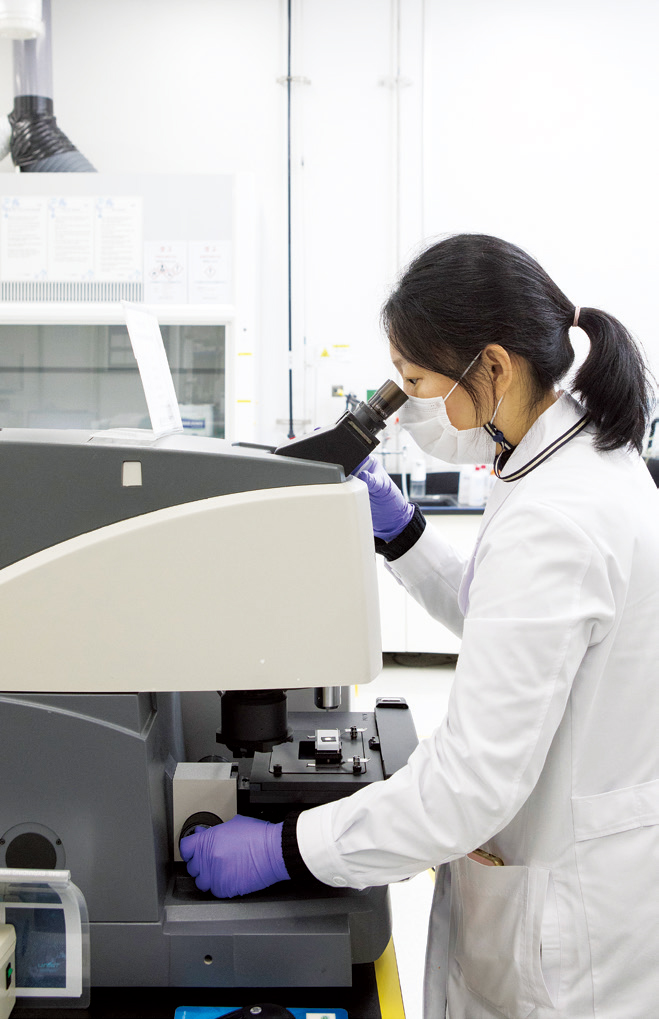
Recently, there have been many requests from researchers to observe a cross-section of a specimen, which can be observed with an SEM. However, this requires a pretreatment process in which a specimen is cut vertically. The problem here, however, is that if the hardness of the material in question varies, the method of cutting it must also be different. Soft materials can also be cut with scissors or a knife, but hard materials such as steel will require a different kind of cutting equipment. Furthermore, even when cutting a soft material, if it is cut with scissors, parts of it may get chewed up in the scissors’ cutting path. Just as when we cut a sheet of paper or cloth, we end up with uneven, torn parts if we do not cut the scissors all at once but divide them several times. In such cases, accurate cross-sectional information cannot be obtained. In other words, if the preprocessing process is not carried out properly, it becomes difficult to obtain good research results.
UCRF is equipped with various kinds of preprocessing equipment that can be used to trim or cut specimens and thereby assist researchers in obtaining accurate research results. Naturally, each preprocessing device is used for a specific purpose, and we are building pretreatment equipment suitable for various materials ranging from polymers and biomaterials to steel. Typical examples of such equipment include the ion milling system and the ultramicrotome: The former irradiates argon (Ar) ions to the uneven parts of a specimen and finely trims them, whereas the latter is a device for cutting polymers or biomaterials by cutting specimens with a diamond knife. Since both instruments make the specimen's cross-section clean and even, they are advantageous for obtaining effective research results.
Although these preprocessing devices are used less than scanning electron microscopes, they are essential for improving the quality of research. Since UCRF can only have some of the equipment, it is working to build an optimal research environment through selection and concentration. We select our equipment based on such criteria as researchers’ demands and requirements, research status, and future value.
In the future, UCRF plans to support research by upgrading the level of SEMs. First, we are considering upgrading our SEMs so that our researchers can use the FIB 3D simulation program to check the 3D structure of synthesized specimens. This is because there is demand among researchers who want to examine the interior of a material when it is synthesized in 3D. Also, as the demand for small-scale analysis has increased, we are considering procuring ultra-high-resolution SEMs with the in-lens type of objective lens (i.e. magnification at the level of a TEM, about x300k or more) or the snorkel type.
Given that the development of research equipment facilitates the development of science, the introduction of new equipment and the upgrading of existing equipment must be carried out steadily to revitalize research and raise the level of the results. UCRF fully sympathizes with these needs and demands and will continue to support UNIST’s researchers proactively.
UNIST Central
Research Facilities